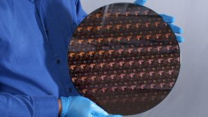
Samsung and IBM Planning a Development in Chip Technology

In May 2021, Samsung announced a development in semiconductor materials that resulted in the development of a device that might postpone the “end” of Moore’s Law and expand the capability gap between China and U.S adjacent efforts in the field of 1-nanometer chips.
The achievement was made possible by a collaborative effort combining the Massachusetts Institute of Technology (MIT), National Taiwan University (NTU), and Taiwan Semiconductor Manufacturing Co (TSMC), the world’s biggest contract maker of innovative chips. At the heart of the achievement was a procedure that uses semi-metal bismuth to enable the production of semiconductors with dimensions smaller than one nanometer (nm).
Samsung and IBM planning a development In chip technology, they have achieved a significant advancement in semiconductor chip technology. The two businesses introduced a novel architecture for stacking transistors vertically on a chip during the IEDM conference in San Francisco, which could substantially enhance power efficiency and performance. The transistors in today’s CPUs and SoCs are flat on a surface, and electric current flows from side to side. However, with the new Vertical Transport Field Effect Transistors (VTFET) architecture from Samsung and IBM, transistors are stacked on top of each other and current flows vertically.
Also read, Oppo Find N Video Teaser and Leaked GreekBench Listing Reveals More Information
In comparison to existing technology, the VTFET architecture allows for a higher density of components on a chip. Moore’s Law states that the number of transistors in a dense integrated circuit doubles every two years. Samsung and IBM are hoping to extend Moore’s Law beyond the nanosheet level while wasting less energy.
According to IBM and Samsung, these characteristics will increase performance or use 85% less power than chips created with FinFET transistors. However, these two companies are not the only ones experimenting with this technology.
According to Reuters, Intel is also testing with processors layered on top of each other. “We’re definitely saving space by stacking the devices right on top of each other,” Paul Fischer, director and senior principal engineer of Intel’s Components Research Group, told Reuters in an interview. “We’re shortening connection lengths and saving a lot of energy, making this not just more cost-effective, but also more efficient.” Intel expects to complete these devices by 2024, utilizing their new “Intel 20A” node with RibbonFET transistors.
Also read, Apple is Not Going to Launch any Foldable Phone Until 2023
PTA Taxes Portal
Find PTA Taxes on All Phones on a Single Page using the PhoneWorld PTA Taxes Portal
Explore NowFollow us on Google News!


